Fedora Electronic Lab (FEL) comes to fix one big problem in the opensource community. This problem is usually unknown to many people or taken for granted.
The problem is : there is no one who provides opensource EDA solutions for the real life. Although it is one problem, it is very complex in itself. In real life, designers use EDA software to design chips or circuit boards. Thereby the designer requires a set of hardware design tools to design his/her chips. However the same set of hardware design tools does not apply for every hardware design project.
Since a hardware design project consists of different types of circuits: Analog, Digital and Mixed Signal, each of these types entails its own design flow and methodologies. Each type requires several different EDA software to successfully design, simulate and verify the designed circuit. Since these types of circuits are incorporated on same die, these circuits should be able to interface each other. Thereby as an EDA provider we should provide our users with EDA solutions that fulfill design flows rather than random EDA software.
After 3 years of hard work, one can define FEL as :
Fedora Electronic Lab is Fedora's high-end hardware design and simulation platform. This platform provides different hardware design flows based on the semiconductor industry's current trend. FEL maps in three methodologies {design, simulation and verification} with opensource EDA software to give a better hardware design experience.
FEL also bridges 2 different opensource communities :
- opensource software community
- opensource hardware community
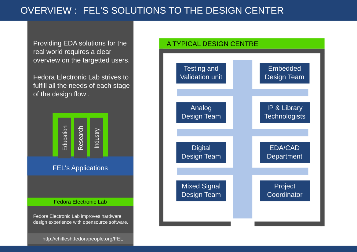
As an EDA provider, we have to know what are the targeting users. Below is a picture describing a typical Semiconductor design centre. This design centre is composed of several design teams and each design team needs to interact with other design team. What is also important here is sharing of data between design teams should be possible. We have worked with several upstream projects to make it possible and other upstream projects have opted industry standard format to make interoperability possible. It is also crucial that the data format from commercial software could be read by opensource EDA software. However this is beyond our reach.
When the design centre receives a project and project specifications have already been established by the marketing team, the project coordinator will have to divide the project in accordance to his/her respective design teams. The EDA/CAD department assists the design teams with the proper EDA software with respect to the project. Each design teams will work with several design tools (at least 5) together with some in-house scripts. These EDA software ensure design, simulation and verification methodologies. After the project have been taped-out and manufactured. The Testing and Validation Unit verifies the chips or circuit boards one by one.
From the Project Specifications till the final validation, FEL strives to satisfy all the needs of the design centre. FEL also provides the design centre with 7 standard cells libraries. Since the semiconductor industry is a highly competitive environment, it is a never-ending process to provide several methodologies to improve hardware design experience.
 We spend our free time for you.